17 System components
The book is still taking shape, and your feedback is an important part of the process. Suggestions of all kinds are welcome—whether it’s fixing small errors, raising bigger questions, or offering new perspectives. I’ll do my best to respond, but please keep in mind that the text will continue to change significantly over the next two years.
You can share comments through GitHub Issues.
Feel free to open a new issue or join an existing discussion. To make feedback easier to address, please point to the section you have in mind—by section number or a short snippet of text. Adding a label characterizing your issue would also be helpful.
Last updated: November 15, 2025
17.1 System components overview
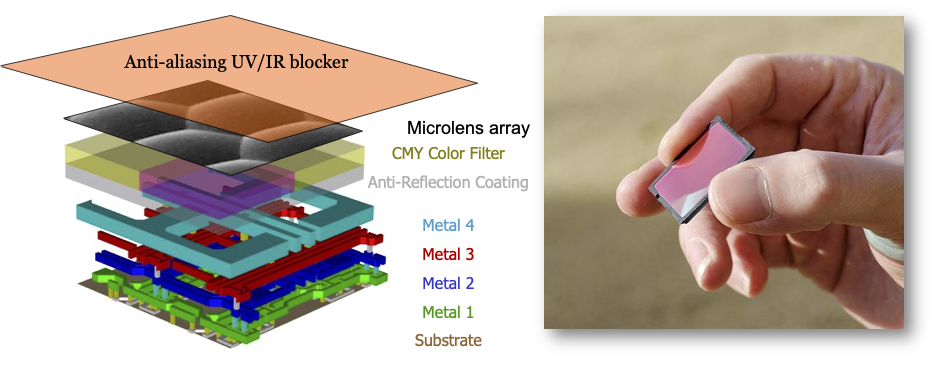
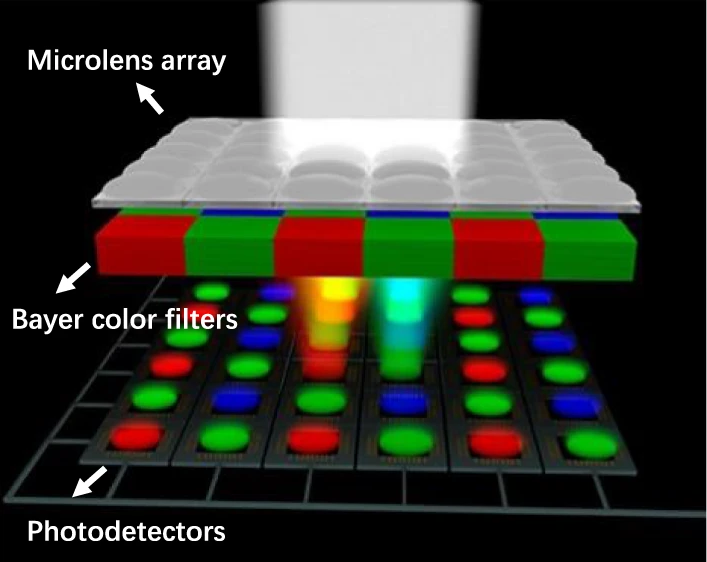
Modern CMOS image sensors combine several carefully engineered layers that work together to capture sharp, low-noise, and color-accurate images (Figure 15.2). Light from the scene passes through (1) the main lens, (2) an optional UV/IR blocking filter that limits the spectrum to the visible range, (3) a microlens array that concentrates and redirects the light toward each pixel’s active area, and (4) a color filter array (CFA) that partitions the visible spectrum into broad bands for color reproduction. Beneath these layers, (5) deep trench isolation (DTI) structures reduce optical and electrical crosstalk between neighboring pixels, while (6) the photodiode converts absorbed photons into charge for readout.
Each element serves a distinct purpose: the microlenses and DTI increase quantum efficiency and preserve spatial detail; the UV/IR filter and CFA shape the spectral sensitivity; and the pixel architecture and readout circuits determine noise performance. In the following sections we describe how these components evolved and how each contributes to image quality.
17.2 Spatial components
17.2.1 Microlens arrays
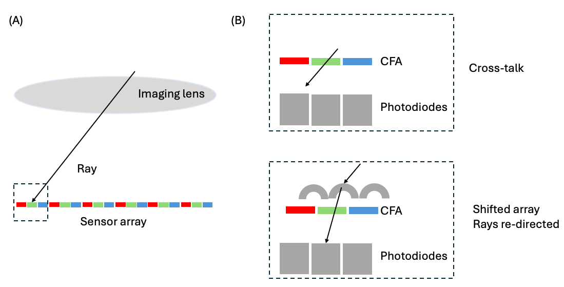
The microlens array is a layer of tiny lenses placed above the color filter array. These lenses serve to redirect the light from the main lens onto the photodiode, increasing the light-gathering efficiency. The microlens also reduces pixel cross-talk. This refers to the case in which light from the imaging lens might arrive at a relatively large angle at the color filter. A ray may end up generating electrons in a pixel that has a different color filter. Over time, microlens arrays have evolved to support additional functions, such as optimizing focus and enabling advanced imaging techniques for light field capture that I describe later.
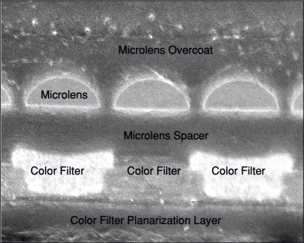
At the center of the sensor array, the incidence of the chief ray from the center of the lens is close to perpendicular to the photodiode array. There, a lens centered above the photodiode works well to simply concentrate the rays. At the edges of the array, however, the angle of the chief ray is relatively steep, say 35 degrees. To redirect the rays toward the photodiode, the microlens and the color filter are shifted laterally. The decentering of the microlens and color filters improves the redirection of the rays so that more light arrives at the proper photodiode, and less light is incorrectly absorbed by adjacent photodiodes.
The microlens was important for classic, frontside illuminated sensors when the path from the lens through the metal layers was quite long and the angle of the chief ray at the edge was fairly large. For large pixels, and the initial sensor pixels were 6 or more microns, microlens technology was quite effective (Hwang and Kim (2023a) Hwang and Kim (2023b)).
17.2.2 Deep trench isolation (DTI)
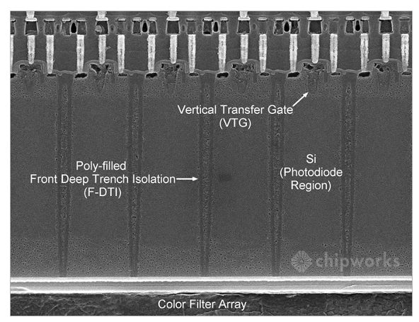
As pixel sizes shrank to around 1.5 microns or less, diffraction effects became more significant. Light entering these tiny pixel apertures would spread out, causing photons to be absorbed not only by the intended photodiode but also by neighboring ones. This led to two main issues: reduced image sharpness due to optical blur, and decreased color accuracy because light passing through, for example, a green filter could generate electrons in a photodiode beneath a red filter.
Deep trench isolation (DTI) technology addresses these challenges. Engineers introduced narrow trenches at the boundaries between pixels and filled them with insulating materials such as silicon dioxide or silicon nitride (Figure 17.3). These trenches act as barriers, preventing light from spreading laterally between adjacent pixels. As a result, DTI improves both spatial resolution and color fidelity in modern image sensors (Han et al. (2020), Tournier et al. (2011), Park et al. (2007)).
17.3 Spectral components
Silicon-based CMOS image sensors are sensitive to photons with wavelengths up to about 1100 nm. In contrast, the human eye detects only a narrower range, from roughly 380 nm to 700 nm. For consumer cameras, the goal is to capture images that look natural to people, so sensors are designed to record light mainly within the visible spectrum. Since human vision uses three types of broadband photoreceptors, most cameras only need to capture three broad spectral bands.
To achieve this, image sensors use two types of spectral filters: one to block unwanted infrared (IR) and ultraviolet (UV) light, and another to divide the visible spectrum into three color channels. The resulting data are processed to produce images that closely match human color perception. In this section, I describe these filters. After reviewing the relevant properties of human vision (Chapter 23), I explain how sensor color channels are processed to render accurate or visually pleasing images (Chapter 26).
17.3.1 UV/IR filters
Most consumer cameras include a spectral filter that blocks wavelengths longer than 680–700 nm (IR) and shorter than 380–400 nm (UV) from reaching the photodiode. These thin UV/IR blocking filters are placed above the microlenses on the sensor (Figure 17.4)1.
Early digital cameras often included an additional laminated layer called an optical low pass filter (OLPF), which slightly blurred the image. The OLPF ensured that light from a point in the scene would be spread over a small area (such as a 2x2 pixel region). This blur was useful because adjacent pixels have different color filters, but their outputs are combined and treated as coming from a single point in the scene. In recent cameras, pixel sizes have become so small that diffraction already spreads the light across multiple pixels (Figure 7.12), making the OLPF unnecessary.
17.3.2 Color filter arrays (CFA)
Below the UV/IR blocking filter, color cameras have a color filter array (CFA) (Figure 15.3). Typically, the CFA consists of three types of filters arranged in a repeating pattern. The smallest repeating unit is called a super pixel. Pixels behind each filter type form a mosaic that samples the image, and together these mosaics create three interleaved color channels. For consumer photography, the most common CFA pattern is the Bayer pattern (1976), which uses two green filters, one red, and one blue in each super pixel (Figure 17.5).
Bryce Bayer worked at Kodak Research Labs and invented the Bayer color filter array.
In the mid-1960s, Bayer’s group worked alongside another team focused on psychophysics and human color perception. Kodak was among the first companies to design and market digital cameras, and he was consulted on how to arrange the color filters. The Bayer filter configuration was designed to mimic aspects of human vision: specifically, he proposed using twice as many green filters as red or blue, reflecting the human eye’s greater spatial resolution to these wavelengths.
In March 1975, Kodak filed a patent application titled “Color imaging array,” naming Bayer as the sole inventor. The patent (U.S. 3,971,065, issued July 1976) became foundational for digital imaging. Kodak typically licensed its patents as a bundle, with the Bayer filter patent being a key part of this portfolio. While it is difficult to assign a specific value to this single patent, it contributed significantly to the value of Kodak’s licensing program, which generated billions of dollars. Despite this, Kodak ultimately struggled to adapt to the digital era (Section 1.2.2).
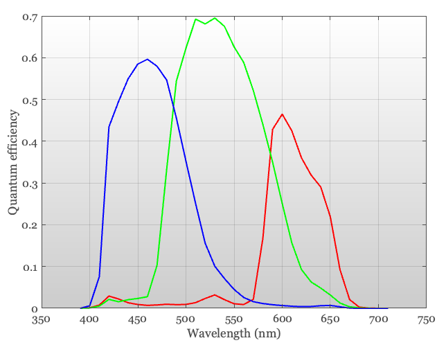
Figure 17.6 shows the spectral transmission of three color filters from a consumer camera. Over the years, the number of different color filters used in color photography has converged onto a relatively small set with common properties (Tominaga et al. (2021)). Different spectral filters and physical methods for sampling the spectrum are used in for other applications, such as medical, scientific, or industrial cameras.
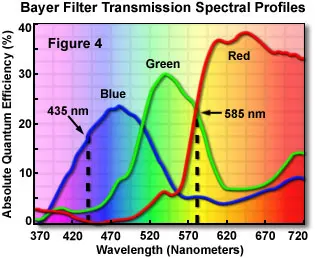
The spectral sensitivity of a color channel depends on the entire light path, not just the color filter. The sensitivity depends on the light transmitted by the lens, the UV/IR filter, the microlens, the color filter, and finally the spectral quantum efficiency of the photodiode. Each of these components can affect the probability that a photon is absorbed; their combined effect determines the overall spectral responsivity of the color channel.
When using a color filter array, we obtain one spectral sample at each position. To represent a color image, however, we represent three spectral samples at each location. Thus, we must convert the data from these interleaved mosaics to create a full-color image by assigning a red, green, and blue value at every pixel location. This process, called demosaicking can be very useful when a sensor has relatively large pixels. In that case, the images are coarsely sampled and the image appearance is significantly improved by interpolating the color channels, essentially upsampling the measurements.
There is a principle we can use when evaluating whether a pixel is ‘large’. The imaging lens has a point spread function (Section 7.8), and if the spread is two times larger than the pixel size we consider the pixel small. On the other hand, if the pixel is equal to or larger than the point spread, we consider the pixel large.
For modern sensors, particularly in consumer imaging, pixel sizes can be quite small, often less than \(1~\mu \text{m}\). This pixel size is smaller than the ideal point spread function of a diffraction limited lens (Section 7.7), and often considerably smaller than the point spread function of the true system. For such sensors many small pixels —and even the entire super pixel- fit within the point spread function. Demosaicking is less critical in this case; we can simply group the measured values of the super pixel into a single point in the RGB image. We will quantify the impact of optics, pixel size and demosaicking for image quality in Chapter 26.
Although these filters block both UV and IR, they are often called IR blocking filters. This may be because the glass in the optics already blocks much of the UV light.↩︎