15 Pixels and sensors
The book is still taking shape, and your feedback is an important part of the process. Suggestions of all kinds are welcome—whether it’s fixing small errors, raising bigger questions, or offering new perspectives. I’ll do my best to respond, but please keep in mind that the text will continue to change significantly over the next two years.
You can share comments through GitHub Issues.
Feel free to open a new issue or join an existing discussion. To make feedback easier to address, please point to the section you have in mind—by section number or a short snippet of text. Adding a label characterizing your issue would also be helpful.
Last updated: November 8, 2025
15.1 Pixels and sensors
I now connect the physics of photon-to-electron conversion to the engineering of image sensor pixels. First, we review how electrons behave in semiconductor materials and how photons create mobile charge carriers (Section 15.2). Then I examine how CMOS pixel architectures (e.g., classic 3T and 4T designs, and their modern extensions) store, transfer, and read out that charge.
Subsequent sections explain how pixel structures have evolved (front-side to back-side illumination, deep photodiodes, stacking, and digital pixels) to improve sensitivity, speed, and dynamic range. Finally, I describe how to model and measure sensor performance (Section 19.1) and how additional on-sensor components—such as color filters and microlenses—shape the captured data (Chapter 17).
The goal of these chapters is to build an intuition that links semiconductor physics to practical design trade-offs in modern image sensors.
15.2 Semiconductors and electrons
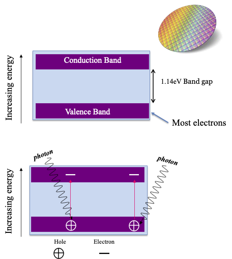
Atoms in a silicon semiconductor are arranged in a crystalline structure, and their electrons occupy specific energy levels grouped into two main bands: the valence band (lower energy) and the conduction band (higher energy). Under normal conditions, most electrons remain in the valence band. When a silicon atom absorbs a photon, an electron can be excited from the valence band to the conduction band (Figure 15.1).
15.2.1 Bandgap
The minimum energy required for this transition is called the bandgap, and it is measured in electron volts (eV). For silicon at room temperature (\(21 \deg C\)), the bandgap is 1.12 eV. Only photons with energy equal to or greater than this value can generate free electrons in silicon.
Without special circuitry, the hole and electron will re-combine. To make an image sensor, we need a method to measure the number of electrons. In a CCD an electric field between the bands prevents recombination. In CMOS electrons are trapped in capacitors placed in the silicon. We explain this circuitry below.
15.2.2 Wavelength effects in silicon sensors
There are several wavelength-dependent effects worth noting about silicon sensors. First, we can calculate the energy in Joules of a photon of wavelength \(\lambda\) using this the photon energy formula:
We can convert from Joules (J) to electron volts (eV) with this formula
\[ 1~\text{eV} = {1.602 \times 10^{-19}}~\text{J} \tag{15.1}\]
A wavelength of 1100 nm has just enough energy (1.12 eV) to transition an electron across the bandgap: Thus, silicon sensors are insensitive to electromagnetic radiation beyond 1100 nm and infrared sensors must use a different material. Second, photons with wavelengths less than 1100 nm have enough energy to excite electrons across the bandgap, and silicon will absorb radiation at these shorter wavelengths. It is notable that the eye does not encode wavelengths below about 400 nm.
Third, the chance that a photon excites an electron that crosses the bandgrap depends on the photon’s energy level. Higher energy (shorter wavelength) photons are more likely to cause the electron to change bands. For this reason, different wavelengths are absorbed at different spatial depths in the material. Short-wavelength photons are much more likely to generate electrons near the surface compared to long-wavelength photons. Conversely, long-wavelength photons are relatively more likely to generate electrons deeper in the material. This depth-dependence on wavelength has been used to create color image sensors (Section 20.5).
15.3 CMOS Pixel: Front-side illuminated
CMOS image sensors use photodiodes—and the photoelectric effect—to measure and store the optical light field at the sensor surface. The key technical breakthrough that enabled CMOS sensors was the invention of circuitry to store and then transmit the photon-generated electrons from the photodiode to the computer.
The photodiode and this circuitry are critical parts of the pixel; there are other essential components as well (Figure 15.2). For example, effective image sensors place a small lens (microlens) above each pixel. Color image sensors place a color filter between the microlens and the photodiode that passes certain wavelengths and blocks others.
Figure 15.2 is a schematic that omits many details. For example, notice the gap between the photodiode and the color filter. In early CMOS imagers, this gap contained many metal lines that carried control and data signals. The metal lines were organized into layers and they are illustrated in Figure 15.3. In the first generation of image sensors the distance from the microlens at the top to the photodiode at the bottom was fairly large compared to the size of the photodiode. In these early pixels, light from the main lens had to travel through what was effectively a tunnel to reach the photodiode.
Pixel architecture has evolved significantly over the years, and there continue to be many novel designs. The most straightforward change is that technology has scaled, enabling pixel sizes to shrink and thus increasing spatial sampling resolution. In addition, the placement of the circuitry and metal lines has changed to below the photodiode; light no longer passes through a deep tunnel. There are other improvements to the circuitry, some experimental, that we will review later in Chapter 20. It is helpful to first understand the concepts behind the classic circuitry, so that we can better appreciate these innovations.
The logical flow of the circuitry is as follows:
- Before image capture, the sensor circuitry resets each pixel, clearing residual charge from previous exposures.
- During image acquisition, the photodiode array collects electrons generated by incoming light; these electrons are stored within the photodiode (3T) or in a nearby capacitor (4T).
- During readout, the circuitry transfers the stored charge to an analog-to-digital converter (ADC).
- The digital image array records the amount of light captured by each pixel.
The role of the other essential pixel components, the color filter arrays and microlenses, is explained in Section Chapter 17. In Section 19.1 I describes how to calibrate and model sensor performance, from the scene light field to image capture.
15.4 CMOS circuits
15.4.1 Three-Transistor (3T) Pixel Design
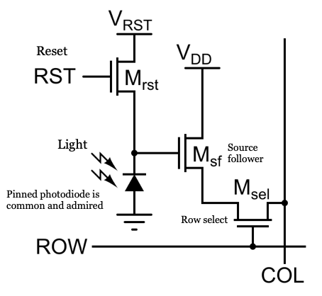
The original CMOS pixel design uses a three-transistor (3T) circuit to store and read out the charge collected by the photodiode (Figure 15.4). Each pixel contains three key transistors: \(M_{rst}\) (reset), \(M_{sel}\) (select), and \(M_{sf}\) (source follower). The \(M_{rst}\) transistor resets the photodiode by connecting it to the supply voltage (Vdd), clearing any residual charge before image capture. The \(M_{sel}\) transistor selects a specific row of pixels, connecting them to the readout circuitry. The \(M_{sf}\) transistor acts as a buffer, transferring the stored charge to the analog-to-digital converter (ADC) for measurement. In most sensors, each column has its own ADC, but some designs use a single ADC shared among multiple columns—a technique known as multiplexing (mux).
Ideally, the photodiode’s response to light is linear, with the number of generated electrons following Poisson statistics. However, the surrounding circuitry introduces additional sources of noise and nonlinearity. For example, the storage capacitor has a limited capacity, so it can saturate at high light levels. The transistors used for readout can also introduce noise and small nonlinearities. Furthermore, variations in pixel properties across the sensor array can cause fixed-pattern noise. In modern CMOS sensors, these nonlinearities and noise sources are typically small—on the order of a few percent (Wang and Theuwissen 2017) -but they can still affect image quality. Careful characterization and calibration are necessary to minimize these effects and produce high-quality images.
15.4.2 Four-Transistor (4T) pixel design
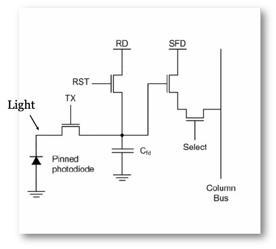
Since about 2000, most CMOS image sensors have used a four-transistor (4T) pixel circuit (Fossum and Hondongwa 2014). The 4T pixel adds two important features: a pinned photodiode (PPD) and a transfer gate transistor (Figure 15.5). The pinned photodiode improves charge storage and reduces noise, while the transfer gate allows precise movement of the collected charge from the photodiode to a storage node called the floating diffusion, which has a capacitance \(C_{fd}\). The other circuit elements—reset, row select, and source follower—remain the same as in the 3T design.
The transfer gate and floating diffusion give the circuit better control over when and how charge is transferred and measured, which helps reduce noise and improve image quality.
Today, the 4T pixel is the standard in almost all high-performance CMOS image sensors, including those found in smartphones, industrial cameras, cars, and scientific instruments.
15.5 Multiplex readout
The use of unity gain amplifiers at the pixel was one important innovation. A second innovation is the way the pixel data are read from the image sensor. In the original CCD devices, the important innovation was to find a way to move the electrons across the silicon array to a single analog-to-digital converter. But the electrons in the CMOS pixels are voltages on a large number of output lines. How shall we convert the voltages on all of these separate lines into digital readout values?
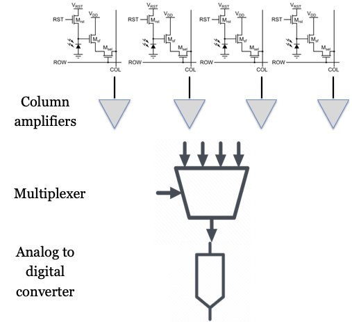
The readout process begins with a control signal sent to a specific row of pixels, activating the row and placing the voltage from each pixel onto its corresponding column readout line. These column lines are connected to amplifiers, which buffer and amplify the signals to ensure accurate transmission. These amplified signals are then passed to an analog-to-digital converter (ADC). The gain settings on the amplifiers, prior to the ADC, are often adjustable allowing gain settings from 1x to 4x.
In most CMOS sensors, ADCs are shared among groups of columns to reduce complexity and save space. This sharing is achieved through a process called multiplexing, where the ADC sequentially converts the analog signals from each column in its group into digital values. Typically, ADCs multiplex signals from 8 or 16 columns, depending on the sensor design and application. Once the data from the active row is fully read out, the control signal moves to the next row, and the process repeats.
15.6 Rolling shutter
So that all of the pixels have the same exposure duration, it is necessary to reset and integrate the pixels in each row a little before the pixels in the subsequent row. Thus, the data in each row is captured a little bit before the data in each of the following rows. This sequential row-by-row readout introduces a temporal pattern known as a rolling shutter into the image data.
Figure 15.7 illustrates the impact of this readout timing. The telephone poles captured in by this CMOS camera from a bullet train in Japan appear slanted. This is because the train is moving quickly, and the rows at the top are captured before the rows at the bottom. During this time, the telephone pole has shifted position to the right. The Japanese are very good at construction: the poles are straight. Very straight.
Technology developments described below enable a different capture method. Some memory is put into each pixel, enabling the sensor to store the pixel value locally. All of the pixels are exposed at the same time, and the data is stored in the local memory. This design, called a global shutter eliminates the rolling shutter effect.
This ISETCam script simulates a rolling shutter. The timing and spatial parameter details of the sensor are included.
15.7 Sensor evolution
There has been a large engineering effort to reduce various sources of noise, including temporal and fixed pattern noise, as well as other limitations in the sensor design relating to color and dynamic range. The engineering effort was supported by the enormous demand for CMOS sensors. In 2020, approximately 6.5 billion sensors were shipped. In 2025, we expect about 13 billion sensors to be produced. That’s a lot of sensors and the demand motivates a lot of engineering. This section covers the evolution of the pixel and sensor design.
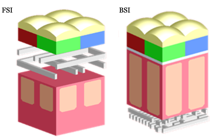
The sensor architecture I have described is known as front-side illumination (FSI). The architecture has the obvious challenge of placing multiple metal layers above the semiconductor substrate (Figure 15.3). Even at the time of the original implementation, it was clear that requiring light to pass through the metal layers to reach the light-sensitive photodiode created many problems.
Additionally, both the photodiodes and their associated circuitry share the same substrate. Requiring the circuitry and photodiode to share space reduced the sensitivity of the sensor. Finally, the original pixels were fairly large, \(6 \mu \text{m}\) or more. As technology scaled and pixels became smaller -many CMOS imagers have pixels as small as \(0.8 \mu \text{m}\) and a reduction in area of \(50x\)- additional problems arose. Different opportunities arose as well.
These challenges, and the huge success of CMOS sensors, were met by a massive, world-wide, engineering effort to improve the system. The evolution of image sensor pixel technology that came from this effort enabled dramatic improvements in image quality, sensitivity, and device functionality. The following sections describe the key milestones that were achieved through academic and industry partnerships. For an authoritative review, consult Oike (2022).
Here is a timeline for the key milestones described in the sections below.
| Technology | Commercialization | Key Benefit |
|---|---|---|
| Front-Side Illumination (FSI) | 1990s–2000s | Simplicity, but limited by wiring obstruction |
| Back-Side Illumination (BSI) | ~2007–2010 | Higher QE, better low-light, smaller pixels |
| Deep Trench Isolation (DTI) | ~2010s | Reduced crosstalk, higher pixel density |
| Deep Photodiode | ~2015+ | Higher sensitivity, dynamic range |
| Stacked Sensor | ~2015+ | Advanced features, compact design |
15.8 Back-side illuminated (BSI)
After years of incremental improvements, engineers developed a new architecture to overcome the limitations of front-side illuminated (FSI) sensors. The resulting design, known as Back-Side illuminated (BSI) CMOS, rearranges the device layers to improve sensitivity. In BSI sensors, the photodiode and wiring layers are flipped; the light no longer needs to pass through the wires.
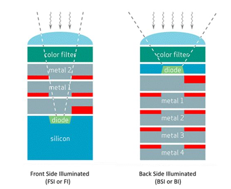
In addition to flipping the order of the silicon and wires, it was necessary to change the thickness of the substrate (Figure 15.9). In the FSI pixel, the photodiode is embedded in a relatively thick layer of silicon. Flipping this structure would require the light to pass through a substantial amount of silicon prior to reaching the photodiode. This is problematic because the silicon absorbs light, and particularly short-wavelength light (Section 17.3). Thus, it was necessary to find a way to thin the silicon substrate and still have a working photodiode and circuitry.
The concept of back-side illuminated (BSI) CMOS image sensors was first proposed by Eric Fossum in 1994 to address the limitations caused by metal wiring obstructing incoming light and to improve sensitivity. While the benefits of rearranging the sensor layers were clear to many, developing a practical manufacturing process proved challenging. It took more than a decade for BSI technology to become commercially viable. OmniVision Technologies was among the first to introduce a commercial BSI sensor, releasing the OV8810 (1.4 μm pixels, 8 megapixels) in September 2008. Sony soon followed, launching the first widely adopted BSI sensors in 2009. See more in this Wikipedia article on BSI.
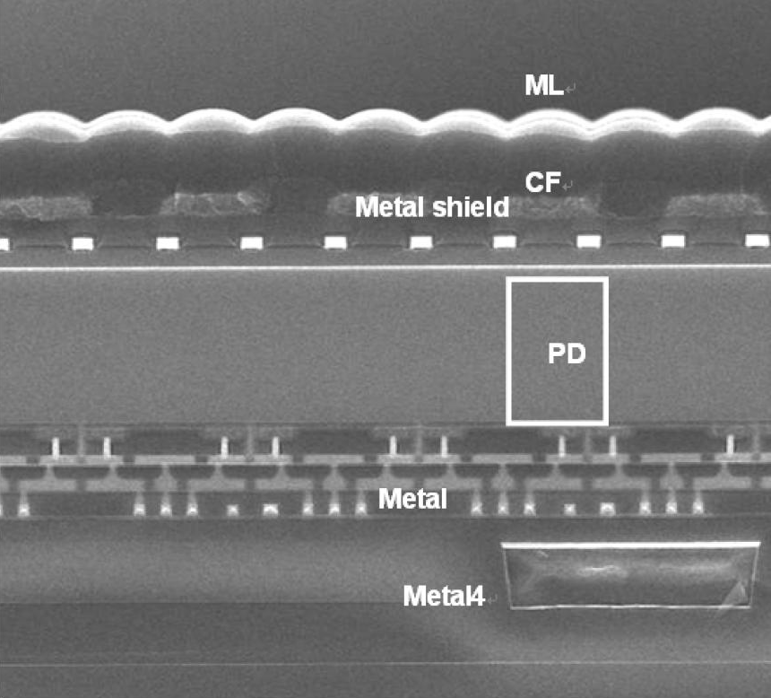
Here is an SEM cross section of an early BSI sensor from Sony. You can see the photodetector (PD) is close to the microlens array level without all the intervening metal layers.
15.9 Deep photodiodes
Figure 15.11 illustrates a further improvement in the BSI design. SK Hynix, Omnivision and other manufacturers recognized that simply flipping the sensor (BSI) improved light capture. But as pixel sizes continued to shrink there was relatively little ability to store electrons. Thus the well capacity was reduced which limited the pixel’s dynamic range (Section 16.3). Moreover, the sensitivity to longer wavelengths, which penetrates deeper into silicon, became a challenge (Section 17.3).
To overcome these limitations, many vendors invented methods to build photodiodes that extend significantly deeper into the silicon (deep photodiode technology). Increasing the volume of the photodiode has two benefits. First, the photodiode can gather more charge before saturating. Second, the photodiode has higher long-wavelength sensitivity.
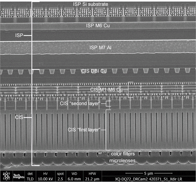
15.10 Stacked sensors
In the original planar technology, photodiodes are adjacent to the transistor circuits within the silicon substrate. Thus, photodiodes must compete for space with the transistors. Reducing the photodiode area means less light efficiency; reducing the transistor size means noisier performance. Youse pays yer money and yer makes yer choice.
The stacked sensor architecture overcomes this limitation by physically separating the photodiode layer from the readout and processing circuitry. In a stacked sensor, the photodiodes occupy one silicon layer, while the supporting electronics are fabricated on a separate layer beneath. This structure maximizes the light-sensitive area (fill factor) for each pixel and enables the use of more advanced, lower-noise circuitry without sacrificing pixel size.
The key enabling technology is called die stacking. The silicon layers are bonded together and electrically connected using two main methods. The original approach used Through-Silicon Vias (TSVs)—tiny holes etched through the silicon and filled with a conductive material (such as copper or tungsten) to create vertical electrical connections.
More recently, Cu-Cu (copper-to-copper) direct bonding has become common. In this method, patterned copper pads on each wafer are precisely aligned and bonded under heat and pressure, allowing for dense, fine-pitch interconnects between the pixel and logic layers. Cu-Cu bonding is ideal for high-resolution, high-speed sensors, enabling features like per-pixel memory used for global shutters which are sold by many companies. TSVs are still used for tasks such as power delivery and global I/O routing.
Stacked sensors have unlocked new capabilities in image sensor design. By separating the photodiode and circuitry layers, manufacturers can improve light sensitivity, reduce noise, and add advanced processing features directly beneath the pixel array. This architecture forms the foundation for ongoing innovation in sensor performance and functionality.
Stacked CMOS sensors build on the BSI CMOS architecture by integrating the pixel array with a separate logic layer. This close integration enables advanced features such as high dynamic range (HDR) imaging, faster frame rates, and on-chip processing—including artificial intelligence (AI) functions.
Some stacked sensors incorporate high-speed DRAM directly beneath the pixel array, allowing for rapid data readout and temporary storage. This architecture made possible innovations like the Sony a9 (2019), which could capture images at 20 frames per second (fps) with a continuous, blackout-free viewfinder experience.
The complexity of the silicon and the multiple functions achieved by these stacked sensors is very impressive; it reminds me of the complexity of the retina. Many important functions for image systems are integrated into these sensing devices, and these functions are typically localized in space. Many other functions are carried out in the central processing units which have access to the image across larger regions of the visual field.
15.11 Digital pixel sensor
The Digital Pixel Sensor (DPS) was a significant parallel development in image sensor technology. The initial ideas were presented in the mid 1990s, at roughly the same time as the APS 3T and 4T circuits were implemented. The APS circuitry included an analog-to-digital conversion (ADC) at the column or chip level. The DPS architecture extended the pixel circuit by including an ADC within the pixel circuit Fowler and El (1995) Udoy et al. (2025).
Digitizing the signal at the pixel had several advantages for high dynamic range imaging, global shuttering and readout speed (El Gamal and Eltoukhy (2005), Kleinfelder et al. (2001), Wandell et al. (2002)). An important feature of the original digital pixel sensors was that the pixel voltage was read non-destructively and repeatedly, say at 1 ms, 2 ms, 4 ms, and so forth. As the photon generated electrons increased in the well, the voltage was sampled. The voltage for each pixel was reported when the pixel had passed one half well capacity, assuring it was much larger than the noise. It would be reported at a time before the well capacity was reached, so that it was below saturation. The information from each pixel was the voltage and the time at which it reached that voltage. Thus, each pixel had its own exposure duration -or put another way, the sensor had a space-varying exposure duration. Pixels in dark regions of the scene had longer exposure times than pixels in the bright regions. We explain the value of this approach for high dynamic range imaging in Section 18.3.
The DPS concept was introduced at an early point in the development of CMOS imagers, and thus it faced significant hurdles in miniaturization. The idea of an ADC on the sensor foreshadowed an opportunity that has arisen as pixel architecture evolves. The stacked pixel structure offers a remedy by allowing the ADC and memory circuits to be placed in a separate layer underneath the photodiode. This enables higher pixel density and broader application of in-pixel conversion. The next generation of image sensors will implement the DPS concept (Fossum et al. (2024)).
El Gamal co-founded Pixim, Inc. in 1998, a fabless semiconductor company that commercialized chipsets for security cameras based on this DPS technology. A challenge for early DPS implementations was the reduced photodiode area in the planar array due to the additional ADC circuitry. This increased the cost of the chip and narrowed the field of potential applications and prevented widespread mainstream adoption for many years. Pixim was acquired by Sony Electronics in 2012.
In 2023 Sony introduced the Sony a9 iii. It has 24.6 Megapixels and a global shutter. The camera can operate at high frame rates (120 frames per sec). It appears to be using a digital pixel approach.
It’s highly probable that Yusuke Oike who worked in the El Gamal group from 2010-2012, played a crucial role in the development and design of the groundbreaking global shutter sensor that is at the core of the a9 III’s capabilities. He has been with Sony Corporation and Sony Semiconductor Solutions Corporation for many years, focusing on research and development of CMOS image sensors, pixel architecture, circuit design, and imaging device technologies. He’s held positions like Senior General Manager of Research Division and is even listed as the newly appointed CTO of Sony Semiconductor Solutions Corporation in a 2025 news release.